As a thin semiconductor substrate, Germanium is used for the epitaxial growth of other materials like gallium arsenide. These materials are essential for multi-junction solar cells, high-frequency electronics, and sensor applications. Furthermore, Germanium's high electron mobility is a key property that is exploited in certain high-speed transistors and integrated circuits.
| Crystal Growth method | VGF or Cz |
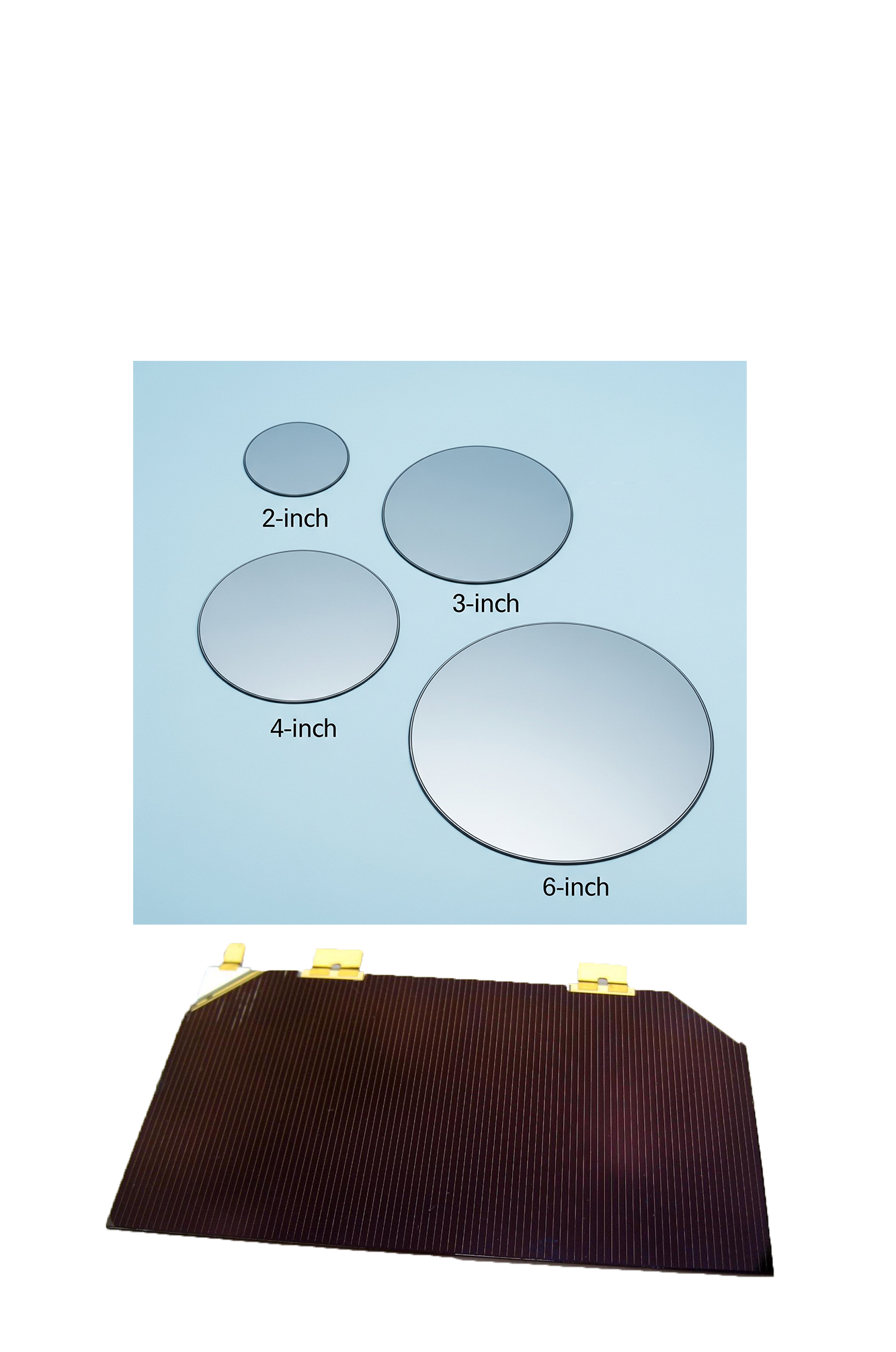
| Diameter | 50.8mm (2”), 76.2mm (3”), 100mm (4”) and 150mm (6”) |
| Thickness | Different options upon request |
| Dopants | Ga for p-type, Sb and P for n-type |
| Resistivity (at 20°C) |
p-type: 0.0005 – 0.5 Ωcm n-type: 0.001 – 0.5 Ωcm IR application: 3 – 30 Ωcm |
| Dislocation density | Depending on orientation, doping and growth method, please ask for details |
| Wafer Orientation | (100), (110), (111), (100) + 6° off (311), (331), (511 etc. … IR standard: mono (111) |
| Surface finish | Options: as-cut, as-ground, polished, epi-ready, standard: front side polished, back side as-ground, double side polished on request |
| Edge finish | rounded |
CORE PRODUCTS, SERVICES AND APPLICATIONS
Our SOLUTIONS
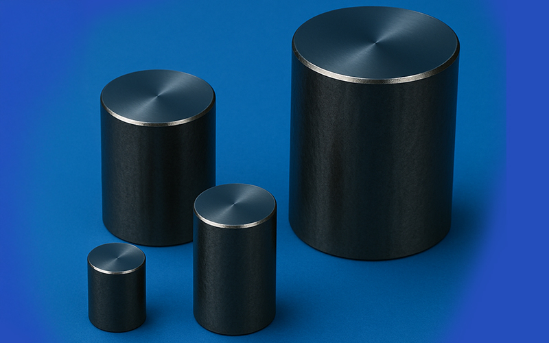
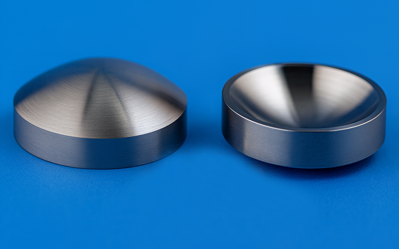
Ge Crystals
Semiconductor and optical Germanium crystals tailored for photonics and sensing applications.
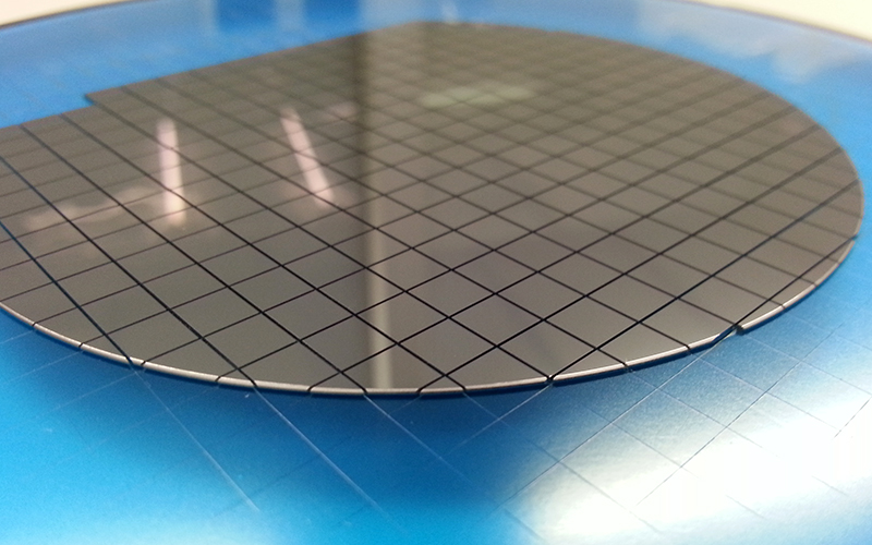
Ge Wafer
High-quality Germanium substrates designed for precision microfabrication and advanced material research.
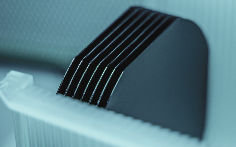
Ge for Monochromators
Precision monochromators and channel-cut crytals for wavelength selection in x-ray and neutron technology.
Ge for Sensor Applications
Wafer structuring and further services for hall-sensors, x-ray sensors and sensor arrays.
Ge for IR Applications
Custom and standard IR lenses and windows optimized for filters and thermal imaging.
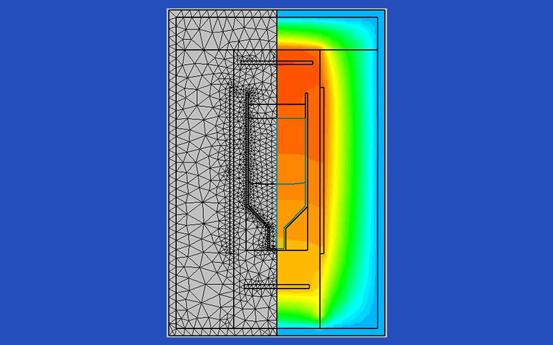
Thermal Simulations
Furnace design and crystal growth modeling by numerical simulations.